The OSI Model 300 Computer Trainer was advertised by Ohio Scientific Instruments in 1976 as a computer designed to introduce individuals to computers and teach them the basics of programming the MOS 6502 processor. The original trainer consists of a MOS 6502 processor, 6810 128 byte static RAM, one bit output latch, switches for entering data, and LEDs for reading the values of RAM.
The trainer was intended as a starter for individuals before moving on to their more advanced Model 400 Superboard system.
I first encountered one of these at VCFE 9.1 in 2014, and was intrigued by the simplicity of the design. I was particularly interested in the operation, and wanted to learn how the switches and LEDs were interfaced to perform the data read/write operations.
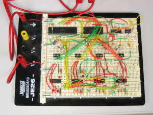
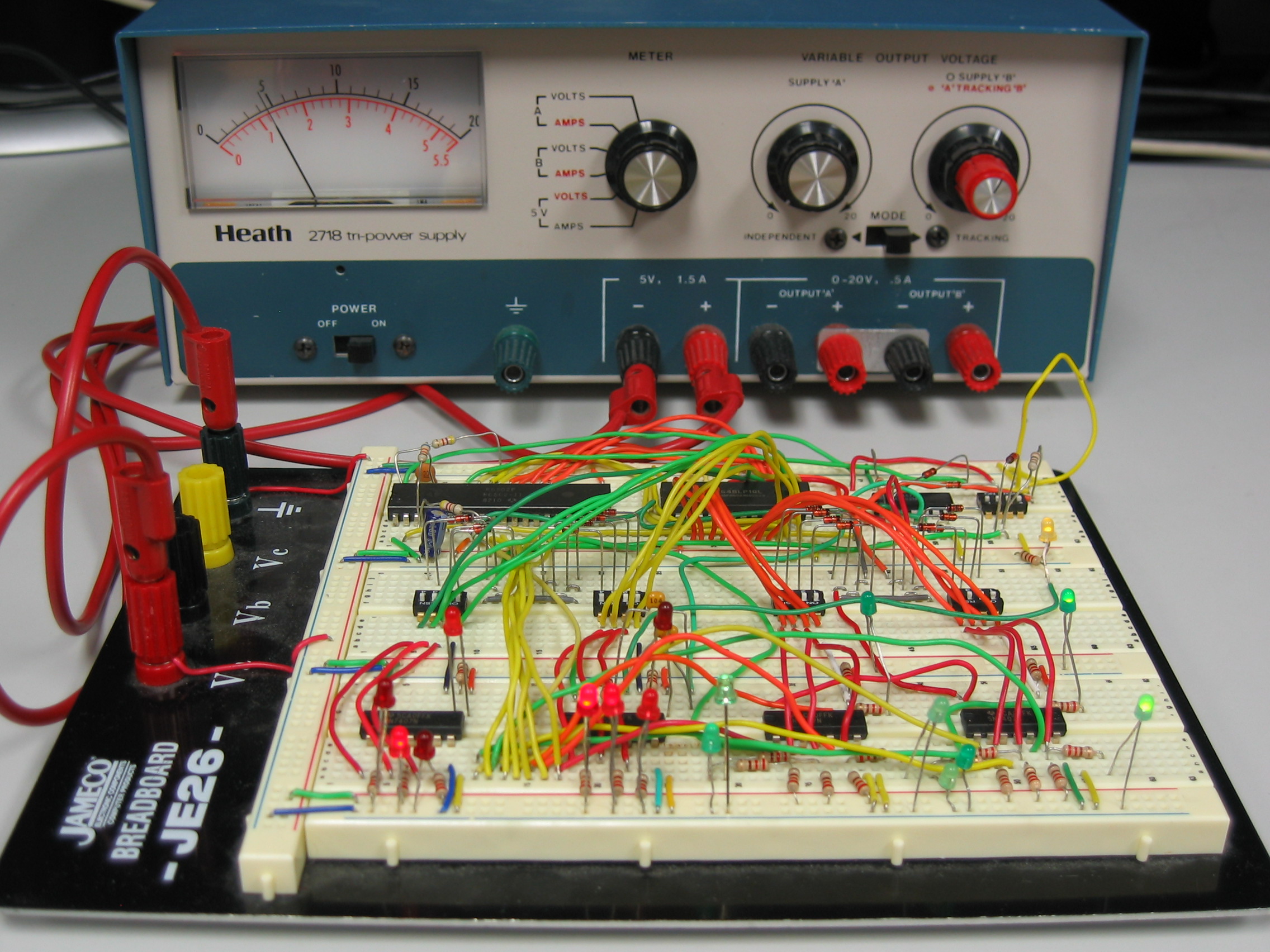
With the assistance of multiple individuals and lots of looking at images, I’ve worked out the schematic for the original and assembled it on a breadboard.
I did make one small change, using a 8k by 8-bit 6264 static RAM chip. As this chip is larger than the original 6810, I added an additional address line for 256 bytes of accessible space. The basic design could be expanded to the full 64k space.
The image shows the results running Experiment 3, which is a basic program that merely loops at location 0. The red LEDs indicate the data, the green the address, and the yellow the run status. If you look closely, you will see the green LEDs represent binary 11, which is because the loop uses locations 00, 01, and 10. The data LEDs represent 01001100, as the 6502 jump instruction is 01001100. The other two locations (01 and 10) both contain 00000000, which represents the location to which the program should jump.
There are several interesting design decisions made to keep the parts count and price down. The first is the usage of a resistor and capacitor to act as the clock. This takes advantage of the internal clock generator on the 6502.
The four buffer chips (7407/7417) provide multiple purposes. For the data lines, they act as drivers for the data LEDs and the run LED. For the address lines, they buffer the lines with the outputs driving both the address LEDs and the address lines for the RAM. The power to the address buffers is only turned on when the RUN switch is active. This in effect tri-states the address lines when the RUN switch is disabled, allowing the switches to drive the address lines without interference from the CPU. This is because the 6502 is incapable of releasing the address lines.
The final chip, a 7402 (quad NOR,) inverts the SYNC line, driving an RC network to stretch it, before it is finally buffered to drive the run LED. Two of the gates form a basic SR latch controlled by the address lines for page 1 and page 2. I used the last NOR gate as an inverter for between the SRAM’s OE and R/W pins.
In the schematic I have generated, the diodes are likely 1N914 or similar with the exception of D35, which is intended for reverse polarity. It is most likely a 1N4001. I have left off the bypass capacitors for clarity. They are likely .2uF on the trainer.
June 19, 2015: I have updated the schematic with a minor correction to the connection of the resistor forming the clock circuit.
Schematic: http://randomvariations.com/wp-content/uploads/2015/05/trainer.pdf
January 1977 Byte Article: https://archive.org/stream/byte-magazine-1977-01/1977_01_BYTE_02-01_Hash_Tables_and_Interrupts#page/n95/mode/2up
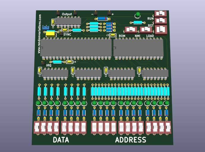 After playing with Kicad, and particularly with pcbnew, I have worked out a PCB design for a “mini” version of the OSI-300 trainer. Only a few changes have been made to the original design.