Apple IIgs 72-pin SIMM memory adapter

4/8MB 72-pin SIMM adapter

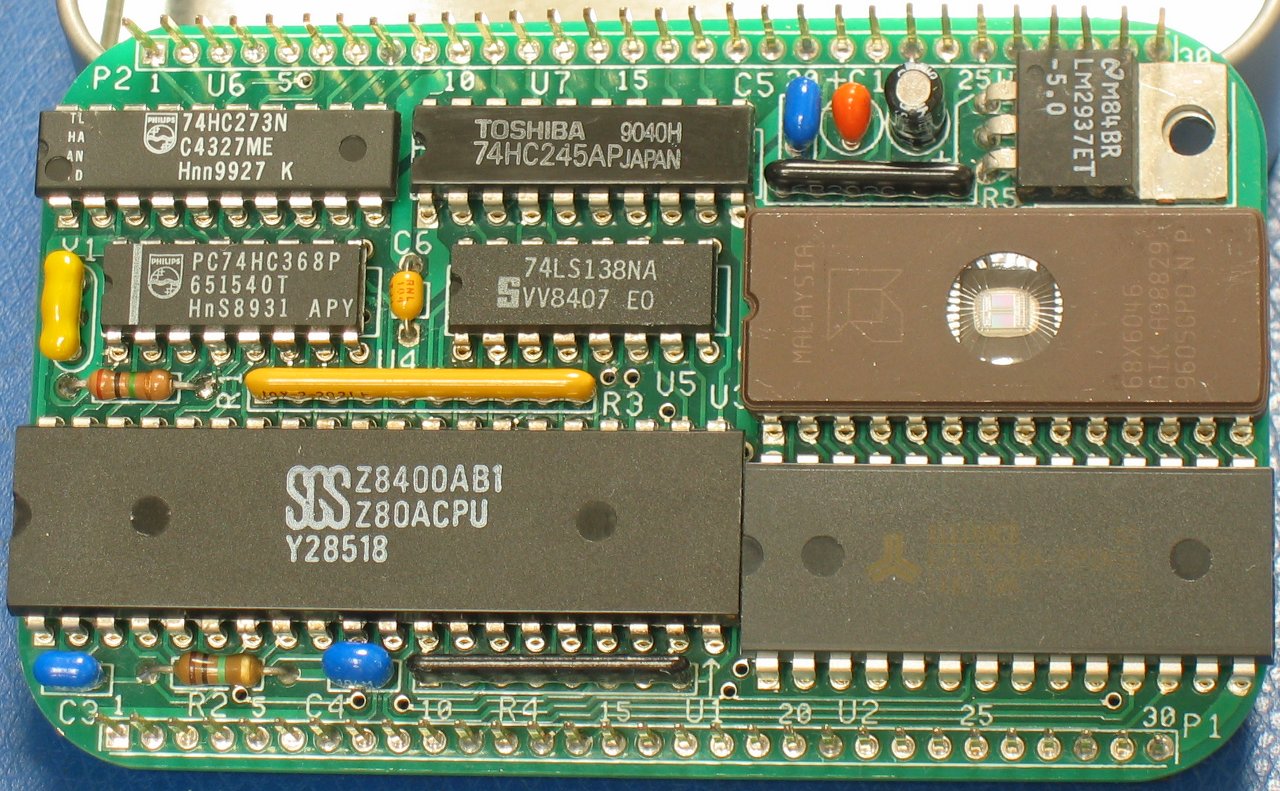
I recently purchased a ROM 01 Apple IIgs with the intention of using it to further my disk image explorations.  While it came with an Apple 1MB expansion card, I quickly realized that it would be useful to have more memory installed.

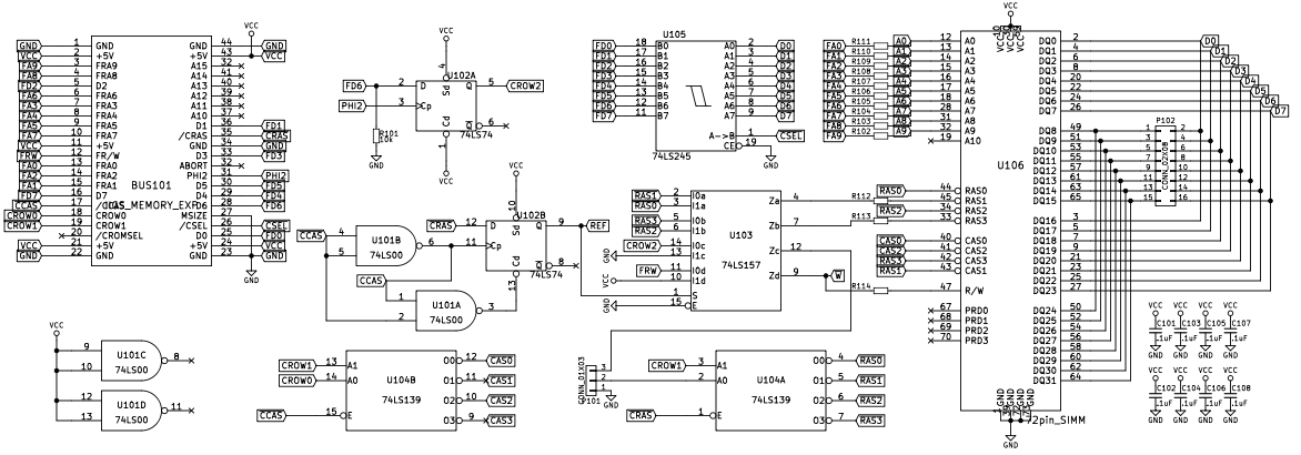
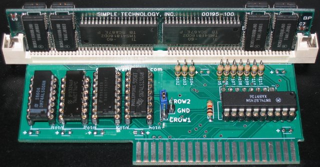
In searching for information regarding the memory expansion capabilities, I came across the postings outlining the RAMGS expansion boards from http://gglabs.us/  In it, the developer notes how it is possible to use FPM DRAM in place of the standard DRAM chips.  I realized that these same chips are those used on standard PC SIMMs.

Analyzing the circuits used by GGlabs, and comparing the memory portion to that of a standard SIMM, I realized that some simplifications can be made.  In particular, the SIMM multiplexes four CAS and four RAS signals to select the byte being read, this means that one of the dual 2:4 decoders can be eliminated by feeding the correct inputs into a single 2:4 decoder.

Due to the way that the IIgs performs memory refresh, it is important to ensure that both 4MB banks be refreshed together.  This is done by using a quad 2:1 mux.  The mux applies the correct input to the 2:4 decoder to ensure that CAS0 and CAS2 (for the first 4MB bank) are selected and that they are routed also to CAS1 and CAS3 (for the second 4MB bank.)  The final 2:1 multiplexer is used to ensure that the write line is high during a refresh, as outlined in the GGlabs reference.

While testing a random assortment of 4MB and 8MB SIMMs that I have collected over the years, I found that this circuit works with EDO SIMMs as well as FPM SIMMs.

4/8MB 72pin SIMM to Apple IIgs memory expansion adapter

OSI-300 Mini Assembly

Assembly of the OSI-300 Mini is fairly straightforward.  I typically start with the shortest height parts, and work up to the tallest.

  1. 1N4148/1N914 diodes D1-D20, D41, D42, and D43
    The black bar on each diode matches the bar on the silkscreen.
  2. 220 ohm resistors R1-R32, R35, and R39
  3. Remaining resistors:
    1. 4.7K ohm resistor R33
    2. 100K ohm resistor R34
    3. 100 ohm resistor R36
    4. 2.2K ohm resistor R37
    5. 4.7K ohm resistor R38
  4. 1N4001 diode D44
  5. .1uF capacitors C1-C5, C7-C9 (Lead spacing: 2.54mm/.1in)
  6. 10pF capacitor C6 (Lead spacing: 5.08mm/.2in)
  7. Sockets (five 14-pin, one 40-pin, one 28-pin)
  8. 3mm LEDs
    The flat edge matches the flat edge on the silkscreen.
  9. Switches
    There are two single-pole double-throw switches wich are different. They are to be used for the run and reset switches. They can be identified by the two slots on the side of the switch body.
  10. Single pin headers
    These should be broken out of the 6-pin breakable header
  11. Jumper
    I usually take a cut lead and bend it into a jumper to bridge the two pads above R34
  12. IC installation
    1. 7417N U1-U4 (buffers)
    2. 6502 U5 (CPU)
    3. 6264 U6 (SRAM)
    4. 7402 U7 (output)
  13. Rubber Feet
    I included two rubber feet to be placed under the OSI-300 Mini. They are too big to fit as-is, but can be cut with a sharp pair of scissors to form four half-circles.

A schematic of the PCB board can be found atminitrainer.pdf

I have found that I can test the board without the CPU and SRAM to ensure that the switches work properly by turning off/on the LEDs with the RUN switch set left.

The operation of the board can be accomplished by following the manual at Dave’s OSI repository

I’ve found that while programming, it is necessary to ensure that the RUN is left and RST is right. To run the program, switch RST left, then right, then switch RUN right, followed by RST to the left.  This sequence ensures that the clock starts properly.

Paul has also pointed out that the reset address used in the OSI manual needs to be adjusted due to the extra address lines.  In place of 7C and 7D, you will want to use FFC and FFD.

Update: at this point due to issues with the postal system I no longer will be mailing kits.  If this changes, I will update this post.

Dumping the WP-2 ROM

As part of my project to run Zork on the Tandy WP-2, I found it useful to dump the ROM and take a peek at what it was doing.  While the Service Manual (available online from Club 100, the Internet Archive, and other places) contains a wealth of information, the code is the definitive place to look for information on how something works.

In order to dump the contents of the ROM, I wrote the below to read each code page, and write it out the serial port.  I compiled it with z80asm from Udo Munk’s z80pack.  I loaded the resulting binary onto the WP-2 by using a drive emulator (dlplus on Linux) and captured the results from the serial port to a file.  I then used an old version of IDA which supported the Z80 to perform the disassembly.

Combining the entry points from the service manual with the disassembly I could follow the code to answer questions regarding the operation of the WP-2 that were not completely clear from the manual.

; dumps all of the ROM banks to the serial port
; sets the serial port to 9600
; compile with z80asm -fb -vl DUMPROM.CO
CHARSENSE	equ		100H
CHARGET		equ		103H

SETLOC		equ		109H
GETLOC		equ		10CH
CURSORON	equ		10FH
CURSORTYPE	equ		112H

CHAROUT		equ		118h
PUTCHAR         equ		1A3H
STROUT		equ		11BH
CLS		equ		11EH
BEEP		equ		121H

RSINIT		equ		140H
GETDATALEN	equ		143H
SENDDATA	equ		146H
GETDATA		equ		149H
RSCLOSE		equ		14CH

CHGSLOT		equ		166H

LINEIN		equ		1A6H

BKSP		equ		008H
LF		equ		00AH
CR		equ		00DH
ESC		equ		01BH

		ORG		0AC00H-8
		DEFB		'PR'
		DEFW		PRGEND-PRGTOP+1
		DEFW		START
		DEFW		0000H

PRGTOP
START		CALL	CLS
		NOP
		NOP
		NOP
		NOP
		NOP
		NOP
		NOP
		NOP
		NOP
		NOP
		NOP
		NOP
		NOP
		NOP
		NOP
		NOP
		NOP
		NOP
		NOP
		NOP
		NOP
		NOP
		NOP
		NOP
		NOP
		NOP
		NOP
		NOP
		NOP
		NOP
		NOP
		NOP
		NOP
		NOP
		NOP
		NOP
		NOP
		NOP
		NOP
		NOP
		NOP
		NOP
		NOP
		NOP
		NOP
		XOR	A
		ld	(CURSLOT),a
		CALL	CHGSLOT		; change to slot zero to start
		ld	hl,0h		; start at zero to read the first bank
		ld	(current),hl
		call	DUMPLOOP
MAINLOOP:
		call	BEEP		; We dumped another block
		ld	hl,4000h	; remaining banks start at 4000h
		ld	(current),hl
		ld	a,(curslot)
		inc	a
		ld	(curslot),a	; bump to next slot
		cp	0Fh		; if slot 15 (IC Card)
		jr	z,DONE		; then we are done
		call	CHGSLOT
		call	DUMPLOOP	; otherwise dump it
		jr	MAINLOOP
DONE:		xor	a
		CALL	CHGSLOT		; change back to slot zero
		xor	a
		ret

DUMPLOOP:	
		ld	hl,084Dh	; 9600 bps, 8n1, no xon, timer enabled
		call	RSINIT
BYTELOOP:
		ld	hl,(current)
		ld	a,(hl)
		inc	hl
		ld	(current),hl
		call	SENDDATA
		ld	a,h
		cp	080h
		jr	nz,BYTELOOP
		call	SENDDATA	; for some reason we have to send
					; another dummy byte before the close
		call	RSCLOSE
		ret

CURRENT		DEFW	00000H
CURSLOT		DEFB	0h
PRGEND

		END


Z80 Membership Card

Z80 Membership Card (Front)

While at VCFMW last year, I spent some time talking with Lee Hart about his ELF Membership Card.  He showed me a new project that he had been working on with some others called the Z80 Membership Card.

Z80 Membership Card (Back)

The base Z80 Membership Card contains a Z80 processor, 32k SRAM, and  32k EPROM, along with the necessary components to get them all working together.

Z80 Membership Card Front Panel

The front panel contains everything needed to interact with the membership card, 16 push button switches and a 7 digit display.  The scanning for the keyboard and display are all done through the same 8-bit input and 8-bit output ports.  Lee has also added components to provide for a serial port as well.

Z80 Membership Card Right Side

In addition to the impressive hardware, the Z80 Membership Card comes with some amazing software which interacts with Lee’s hardware design.  The software provides a full interrupt driven monitor which operates the front panel.

Z80 Membership Card Left Side

In addition to scanning the keypad and operating the display, it implements a 9600 baud serial port in software!  The monitor provides for the ability to view/change memory, view/change registers, single step programs, and upload code to memory using the X-modem protocol.

Running Z80 Membership Card In Altoids Tin

Oh, and it lets you do this even while running your own code at the same time!

Lee’s Z80 Membership Card page can be found at:

http://www.sunrise-ev.com/z80.htm

Assembly of the membership card was straight forward, Although I did use a few techniques to get it to fit into the Altoids tin with the lid closed.

To start with, I purchased and used socket pins for all the chips.  The socket pins are almost (but not quite) like having the chips soldered directly to the board.  They allow for enough space between the boards that it isn’t necessary to trim the leads on the front panel as close as it would be required without them.

I then needed to trim the header on the left side.  While the right side has space for holes for the header to extend up into, the left side is too tight.  I trimmed off enough that the pins did not make contact with the front panel.  In hindsight, I could have left the four pins that pass through the corresponding two plugs long.  The body on both headers needed to be shifted to form the two feet along the sides on the bottom.  Carefully sinking the pins into the body prevents shorting to the surface upon which it sits.

The header for power and the serial lines also needs to be installed properly.  I pushed the leads through the plastic body to ensure the correct distance on top (approximately 7mm) and then soldered them in place.

While it took more than a few hours to assemble, I went slowly and carefully to ensure that it would fit properly in the tin.

Mini OSI-300 Parts List

IMG_9007_800x600

The final tally of parts is:

  • 1x R6502 NMOS 6502 CPU
  • 1x 6264 8k x 8 SRAM
  • 4x 7417 Hex Open Collector Buffer
  • 1x 7402 Quad NOR Gate
  • 21x 3mm red LED
  • 23x 1N914/1N4148 diode
  • 1x 1N4001 diode
  • 1x 100 ohm 1/4W resistor
  • 34x 220 ohm 1/4W resistor (I used 1/8W)
  • 1x 2.2k ohm 1/4W resistor
  • 2x 4.7k ohm 1/4W resistor
  • 1x 100k ohm 1/4W resistor
  • 8x .1in (2.54mm lead spacing) .1uF capacitor
  • 1x .2in (5.08mm lead spacing) 10pf capacitor (G0P/NP0)
  • 1x 40pin socket (if desired, turned pin preferred)
  • 1x 28pin socket (if desired, turned pin preferred)
  • 5x 14pin socket (if desired, turned pin preferred)
  • 6x breakaway header, single male pin
  • 24x 4.3mm x 8.6mm SPDT switch (C&K OS102011MS2QN1 or Jameco SS12D02)
  • 1x 6.8mm x 8.6mm DPDT switch (C&K OS202011MS2QN1 or SS22D07)

The mini trainer requires a 5v 1Amp supply to operate, although it does run fine from four AA batteries.