Operating Firmware

Firmware Dump
Firmware Dump

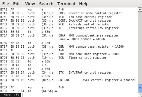
With the correct configuration on the logic analyzer, I was now able to capture the bytes from the firmware as they were checked by the CRC routine.

With a depth of only 1024 bytes, this took some time, but each capture was printed to my laptop.

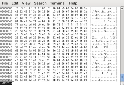
A small script later, and I converted these into a binary dump of the firmware for disassembly.

Even though this didn’t give me the start-up firmware, it did give me useful tools to build that firmware as I captured traces with the logic analyzer.  As I worked my way through the initialization sequence, each trace performed was saved to the laptop, and all the traces were merged together to create an image that could be used concurrently in a disassembler.

Finally, I worked my way down through the initial sequence of keys used to navigate to the upload and download routines.  At this point, the terminal was displaying a prompt asking if I wanted it to send or receive the firmware.

Disassembling Code

Manual DisassemblyInitially, I sat with the logic analyzer, entering each address and byte into a text file, as I followed the start-up sequence of the credit card terminal.  This was a time consuming method, but it gave me excellent training into how the logic analyzer and the credit card terminal worked.

After all, learning was what this project was about!  While doing things “the hard way” is often difficult, it tends to make for a much more rewarding and memorable experience.

As I progressed through the code and grew more experienced, I switched to having the logic analyzer “print” the data recorded through a serial port to my laptop.  This was considerably easier than retyping each byte.  As I followed the normal start-up sequence, I made a very useful discovery.

The terminal ran a CRC check on the firmware stored in flash!


Logic Analyzer Connection

Logic Analyzer Connection

This image shows the final results from carefully tracing the pins from the flash chip back to the other chips in the credit card terminal.  Through this connection, I was able to view the address and data lines as they were connected to the flash chip, along with the important select lines.  I also added connections to the write line and chip enable lines for the main memory.   Exposing these connections would give me a method of capturing the data not only from flash, but memory as well.  The extra signals would make it possible to differentiate between the accesses to the two chips.

With this in place, I was ready to start.  I configured the logic analyzer to store the data and address lines when the flash or memory was accessed, along with the read/write status line.  I set the logic analyzer to run mode, and inserted the plug to power up the credit card terminal.

The results were immediate.  There on the screen was the code currently running, starting at address 0.  The following bytes were the program as it proceeded to initialize the hardware.

I had a long task ahead of myself, but, at least now, I could see inside the system to visualize how the terminal operated.

Verifone Omni 396 Flash

Flash, SRAM, PALs
Flash, SRAM, and PAL chips

This image shows the flash chip in the upper right.  The memory chip is shown on the lower left and the two PAL chips appear on the lower right.

As the flash chip holds the main program of the terminal, I needed to find some way to obtain the contents.  Removing the chip itself and reading it in a programmer was an option, but risky and requiring tools I do not have.  Removing it would also leave me with the task of soldering the chip back into place.

I realized that the device itself was programmable, and, thus, must hold some code inside to reprogram the flash.  I needed to target that procedure.  First, I would need to obtain the protocol to initiate and complete the reprogramming.

Verifone documents the button sequence required to access the local operating system and program one device from another, but not the transfer protocol used between the devices.

I would need the assistance of another tool to obtain the current running code and view what was happening within the device in order to make further progress.

Fortunately, I had just purchased cables and pods for my logic analyzer, which was to be of significant assistance in this entire process.


CP/M running on a Credit Card Terminal

CP/M on Verifone Omni 396

As demonstrated at VCFMW 9.0, this is the Verifone Omni 396 credit card terminal running CP/M.

After reading about Mozart’s Credit Card, I thought that a credit card terminal would make an excellent platform to use for doing something unusual or interesting.   At the time, I didn’t realize how much I would learn while exploring this device.

I started by examining the various credit card terminals available.   Fortunately, many of the sellers list the processors, memory sizes, and capabilities on their web pages.  I have written software for the Z80 many times in the past, and it was used in Verifone’s Tranz line.  A bit more digging and I found this website, which shows the internals of the Omni 395.

The Omni 395 has a Z180 CPU, 512K of memory, 128K of Flash, two RS-232 ports, and a PIN Pad/barcode port.  Like the Tranz 330 used in Mozart’s Credit Card, it had what appeared to be a socketed flash chip, and looked easy to decipher and reprogram.

Looking at images of the outside of the Omni 396, it didn’t look too different.  It still had the same Z180, 512K SRAM (battery backed,) 128K of Flash, and ports on the back.  Given that there was only a small difference in the model numbers, I felt that the components inside should be similar.   As a result, I purchased one and waited for it to arrive.

The first thing I did was to open it up.  I took one look and my heart sunk.  Unlike the Tranz 330, the Omni 396 had surface mount flash with very tiny pins instead of a socketed EPROM or flash chip.

 Obviously, this posed a slightly greater challenge than I had anticipated!