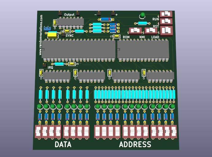
 After playing with Kicad, and particularly with pcbnew, I have worked out a PCB design for a “mini” version of the OSI-300 trainer. Only a few changes have been made to the original design.
The primary adjustment is to swap a 6264 SRAM for the original 128 byte 6810 SRAM. This provides for 8k of space, and allows for more flexibility in that it will also accept a 62256, or with a trace cut and wire adjustment, a 6116. This also permits the replacement of the SRAM with an NVRAM.
I also added 5 additional switches to the address bus. This uses 5 gates on the 7417 open collector buffer chips, which were originally unused. With 12 address bits, 4k is available for programming.
Nice PCB layout, Christopher.
May I ask how pressing reset affects the output flip-flop when accesses to the vector in page $FF set the A8 and A9 address lines to ‘1’?
With 4K of addressable RAM mirrored across the 64K address space, wouldn’t access to RAM in pages x1..x3, x5..x7, x9..xB, and xD..xF also affect the output flip-flop?
Cheerful regards, Mike
Mike,
I don’t have the breadboard version handy at the moment. However, as the gates form an s-r latch, having two ones as an input is technically invalid. In theory, both outputs should be set to zero until the invalid state is changed to one of the valid ones.
Yes, accessing the other pages will affect the output of the flip-flop as well. When designing the PCB, I considered adjusting the set and reset lines to move them outside of the stack and lower pages. However, I decided to try and keep it such that the original experiments can be used as they are outlined in the manual.
It is a simple matter to cut the two traces to the 7402 and add wires to the upper address pins.
That sounds great! And it looks also great!
Any plans to publish your PCB design?