I recently received the boards I designed from the manufacturer. They were very well done, even with the tight tolerances required to line up the various components.
Additionally, the parts I ordered to assemble the board arrived as well, and I set to assembling the board.
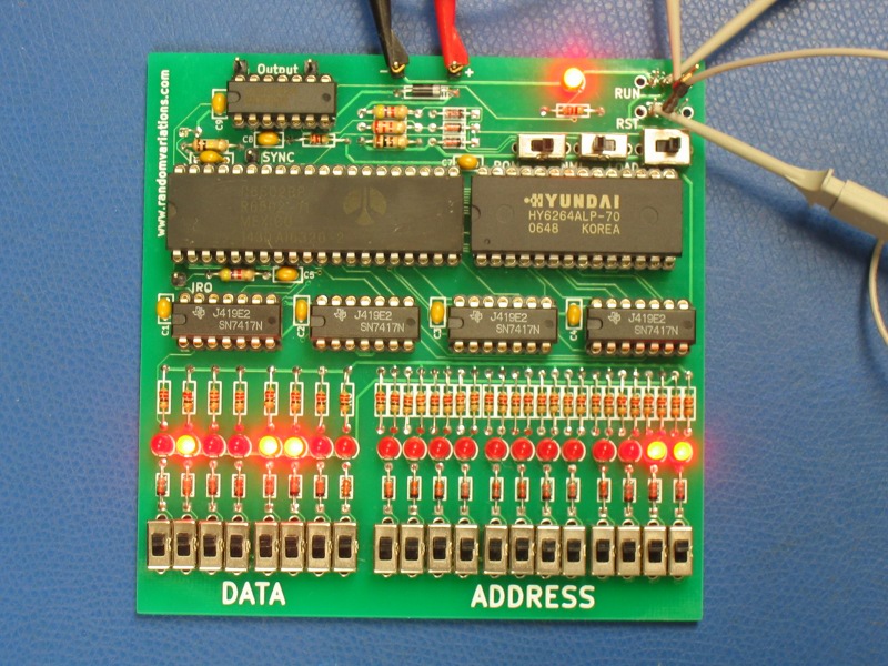
After a few hours of soldering, I was able to come up with the attached image. I ran into only two issues, one with the design, and one with the parts.
The schematic I drew had an issue with the connection between the resistor and capacitor that form the clock circuit. After a single trace was cut and a short piece of wire was attached, I had a working clock.
The other issue I ran into involved the switches in the RUN and RST positions. Both of these switches switch a signal between power and ground. While the switches I picked were supposed to be non-shorting, they appear to briefly short when switched. As a result, power is connected to ground, and the contents of the SRAM are lost. I will try a different manufacturer and see if their switches perform better.
To avoid this, using a pull up or down resistor would be a better design. I wanted to keep as close to the original design as possible.
The image above shows the board running a simple JMP 0000 loop at address 0000. The data LEDs represent 01001100, or 4C in hex, the command for a jump. The address LEDs represent 00000011, or a merge of addresses 0, 1, and 2. While the LEDs are flashing, they are doing so too quickly to see.