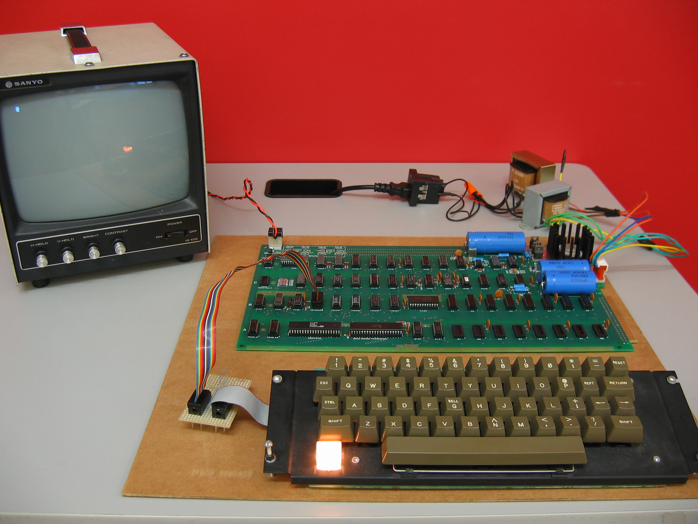
Many years ago, I worked on repairing an Apple 1 computer. At the time, I needed a keyboard and came up with a simple wire wrapped circuit to translate the signals from the Apple II keyboard connector to that expected by the Apple 1 computer.
The Apple II uses the following connection:
       +---| |----+
   +5v | 1     16 | NC
Strobe | 2     15 | -12v
~Reset | 3     14 | NC
    NC | 4     13 | Data 1
Data 5 | 5     12 | Data 0
Data 4 | 6     11 | Data 3
Data 6 | 7     10 | Data 2
   Gnd | 8      9 | NC
       +----------+
The Apple 1 uses the following connection:
       +---| |----+
~Reset | 1     16 | +5v
Data 4 | 2     15 | Data 8 (connected to +5v)
Data 3 | 3     14 | Strobe
Data 2 | 4     13 | NC
Data 1 | 5     12 | Clear Screen (switch to +5v)
Data 5 | 6     11 | -12v
Data 6 | 7     10 | +12v
Data 7 | 8      9 | Gnd
       +----------+
Wiring the two devices together was easy, with one exception. The Apple II keyboard has no switch for clearing the screen. Rather than alter the keyboard, I left two wires exposed for the +5v and clear screen connections, which clear the screen when touched gently together.
Wendell Sander has instructions on how the Apple II keyboard can be wired to the Apple 1 computer’s keyboard input, as well as how it can be modified to use the repeat key as a clear screen key.
For those interested in a board they can simply purchase and use, VintageMicros sells a small adapter board, which includes a clear screen button.
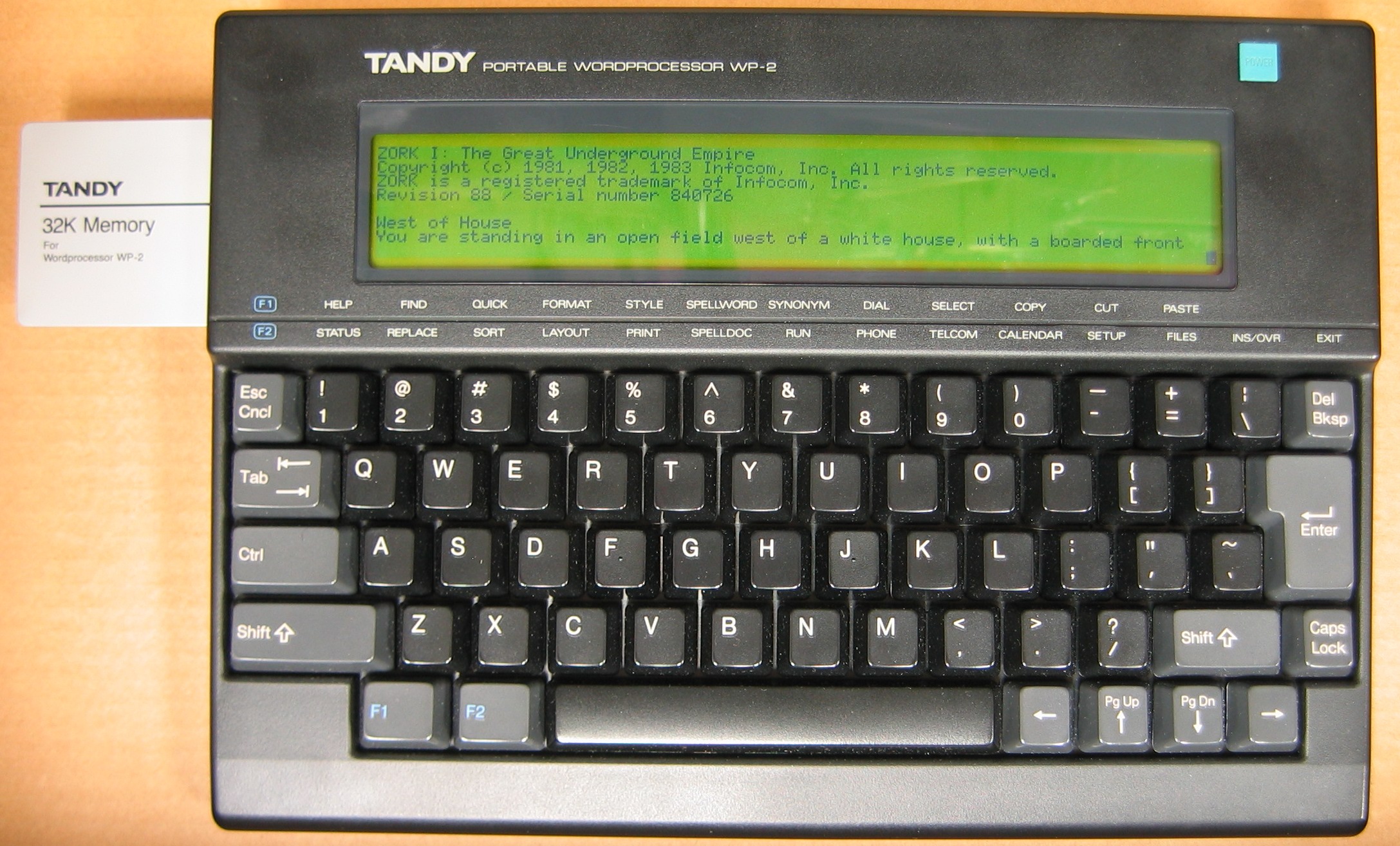
A number of years ago I stopped off at a garage sale and picked up a Tandy portable wordprocessor WP-2. I didn’t do anything with it at the time, but set it aside for further analysis. Late this spring, I came across it on a shelf, and pulled it out to take a closer look.
The WP-2 is based on the Z80 processor and contains 256K of banked ROM, 32k RAM, an 8 character by 80 column display, serial port, cassette port, and printer port. It also has a slot intended for extra RAM and ROM cards. Inside, it has a socket for additional memory. Most individuals added a second 32K ram chip, but 128K chips work as well. The data in RAM is preserved in memory by a small coin cell battery. The word processor normally runs for 20 hours off of 4 AA batteries.
The WP-2 serial port was intended for two purposes. The WP-2 has a terminal program built into it, but will also connect to the same floppy drives that were used on the Model 100 and Model 102. The Model 100 community has come up with software to emulate these drives, which proved to be extremely useful.
Some searching pulled up the service manual for the WP-2. Unlike many service manuals of today, this one included a huge wealth of information. Additionally, it appears that the original developers (in this case Citizen) had intended for the WP-2 to be expandable. The service manual includes schematics, memory maps, and a description of the ROM entry points for procedures such as clearing and writing to the screen, operating on files, and accessing the additional memory banks.
In short, it was a treasure trove for the tinkerer!
As I considered my options, I looked at the core pieces of the device. It had a keyboard, decent sized text display, 128K of built-in mass storage, 32K of RAM, and a floppy drive. In my case, I would emulate the floppy drive with my laptop. To me, a text adventure game would be a natural fit.
My own experiences with the Infocom games and their portability came to mind. The early game files all fit within 128K, and use a text only output format. The game interpreters themselves use only a fraction of the 32K of RAM, and automatically page in information as needed.
The next step was to try and find an interpreter that I could adapt to the WP-2. I explored adapting the CP/M based interpreter, as well as others, but they were all tightly tuned to the systems upon which they ran. However, I came across ZXZVM, which is written in a portable manner. It already runs on the Spectrum, Spectrum +3, and Amstrad systems. Source was available, as well as a brief porting guide.
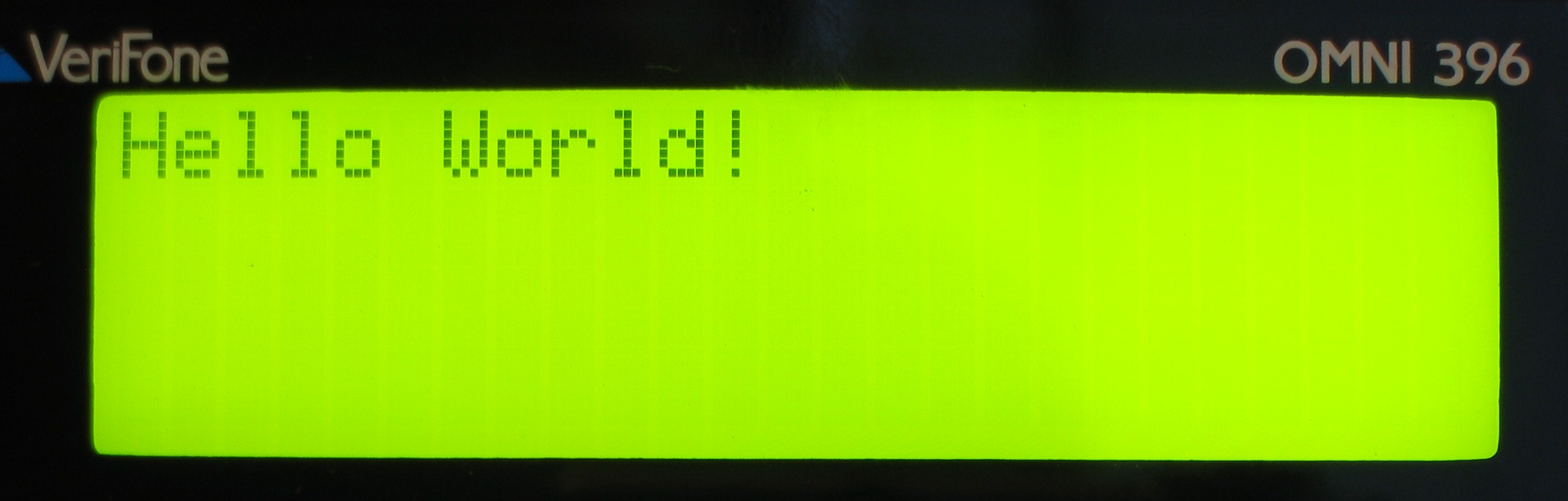
My initial attempt at a program to write hello world to the screen was successful, and led to other small routines. One of these was to dump the contents of the ROM to the serial port. I could use this with a disassembler and the service manual to obtain a clear idea as to how the internal routines worked. With the source to ZXZVM, a basic idea of how to use the internal routines, and a disassembly for a more detailed view of them, I was ready to start.
I started by breaking the large Infocom story file into smaller pieces and then loading them into the extra 128K of extra RAM. This space is normally used for files, but I wanted to just store the raw data there. ZXZVM includes routines to read/write each byte from the story file and the virtual machine’s memory.
Once the virtual machine was able to obtain the story data, it needed a mechanism to read the keyboard and write to the screen. I was able to use the internal routines to do most of the work for this, although they needed some fine tuning to ensure that they fit the expectations of the interpreter.
In the process of adjusting the interpreter, I removed the code that handled later version games. Given the small screen size, and additional game size, it wasn’t needed and the removal provided additional space in main memory.
At this point, with some polishing, I had a basic interpreter running.
However, I was still missing a key element required for some of the games. I needed the ability to save and restore the game.
After searching, I came across and purchased one of the few 32K RAM cards that Tandy produced, and added it to my WP-2.
At this point, I added the additional code to save and restore the game files to the external memory card. I found that I could save only two games to the card, but that the same code could be used to save to a virtual floppy drive if the system was attached to my laptop.
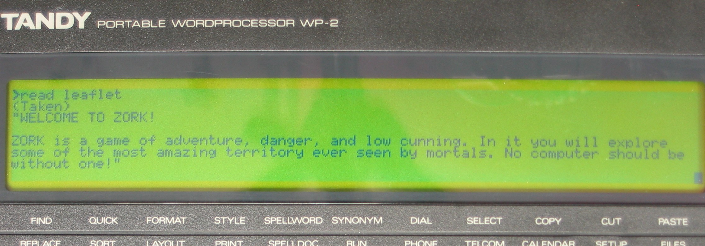
Tandy WP-2 Zork Leaflet
The net result is an extremely playable version of the Infocom interpreter. I have been able to play games such as Zork and Planetfall to completion without issues. The battery backup for the memory makes it just like picking up a book, to play for a while, and then put away until later.
As the leaflet in Zork 1 says, “No computer should be without one!”
While restoring one of my vintage computers, I needed to replace the original PROM chips that were missing when I obtained it. The original chips were MMI 6301-1J parts, which are extremely difficult to find with the correct markings. In order to use vintage parts of a similar age, I located Texas Instruments SN74S287 PROM chips with reasonable 1976 date codes from a seller on eBay.
I expected that these would use the same programming methodology used for the National Semiconductor parts of the same number. Unfortunately, it appears that while Texas Instruments used the same base part number, they use a different programming technique.
As none of the programmers that I had available to me allowed me to program the chips that I purchased, I was forced to build my own.
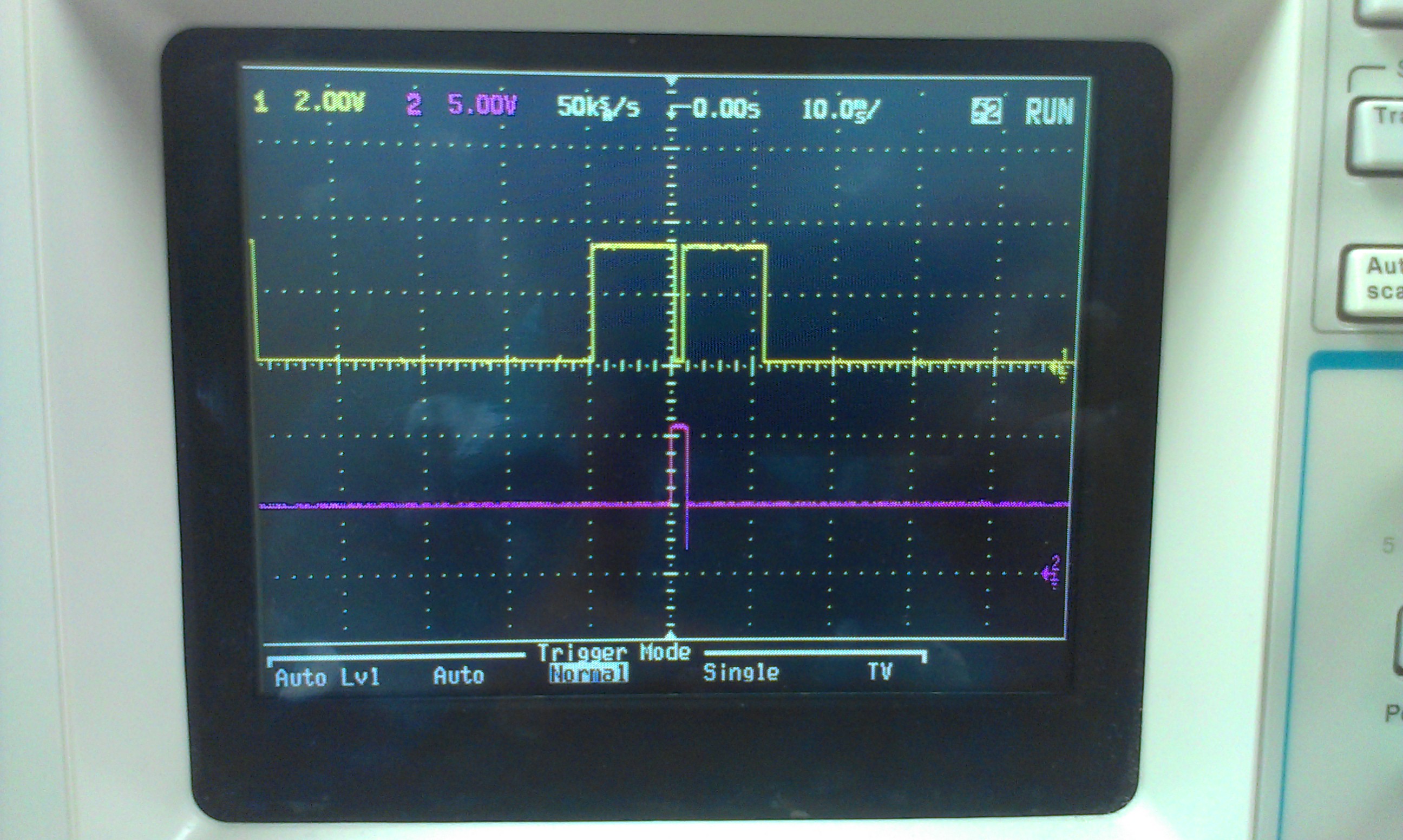
I searched extensively for as much information regarding these parts as I could find. Basically, the programming steps are the following:
SN74S287 Chip Select (top) and Programming (bottom) Pulses
Select address to be programmed
Select single bit to be programmed
Apply 10.5v to Vcc
Select chip(active low)
Wait 10ms for fuse to blow
Deselect the chip
Reduce power back to 5v
Repeat for each bit to be programmed
The timing involved with this is critical. If the pulse is too short, the fuse may not blow properly. If the pulse is held too long, the part could be damaged. Additionally, the intervals between steps must be matched to the data sheet, or the programming mode will not be activated and the chip or programmer could be damaged.
Some of the designs I found were merely a set of address and data switches with a push button to apply 10.5v to Vcc. While this may work sometimes, it would likely result in a number of bad chips, which was discovered by the users. I only had two of the chips, and I needed both of them. If I had a bad burn, I would have to purchase new chips and wait longer to complete my project.
During my research I found that these parts are similar to the MH74S287 by TESLA and use the same programming method. There are a number of articles regarding the programming of the TESLA parts, although most are not written in English. Fortunately, the schematics were easily recognizable!
As a side note, it appears that while the TI SN74S287 programs zero bits, the TESLA MH74S287 appears to program the bits to be one. If you attempt to replicate this with the MH74S287, please consult the data sheet!
My first attempt at a programmer involved the column of 74LS123 retriggerable monostable multivibrators as one-shots on the right in the image above. It worked to create the necessary pulses, but, even after adding additional components to eliminate bouncing of the push button, the circuit was not as reliable as I desired. Using it would have required manually setting the address and data bits, greatly increasing the amount of time to program the entire chip.
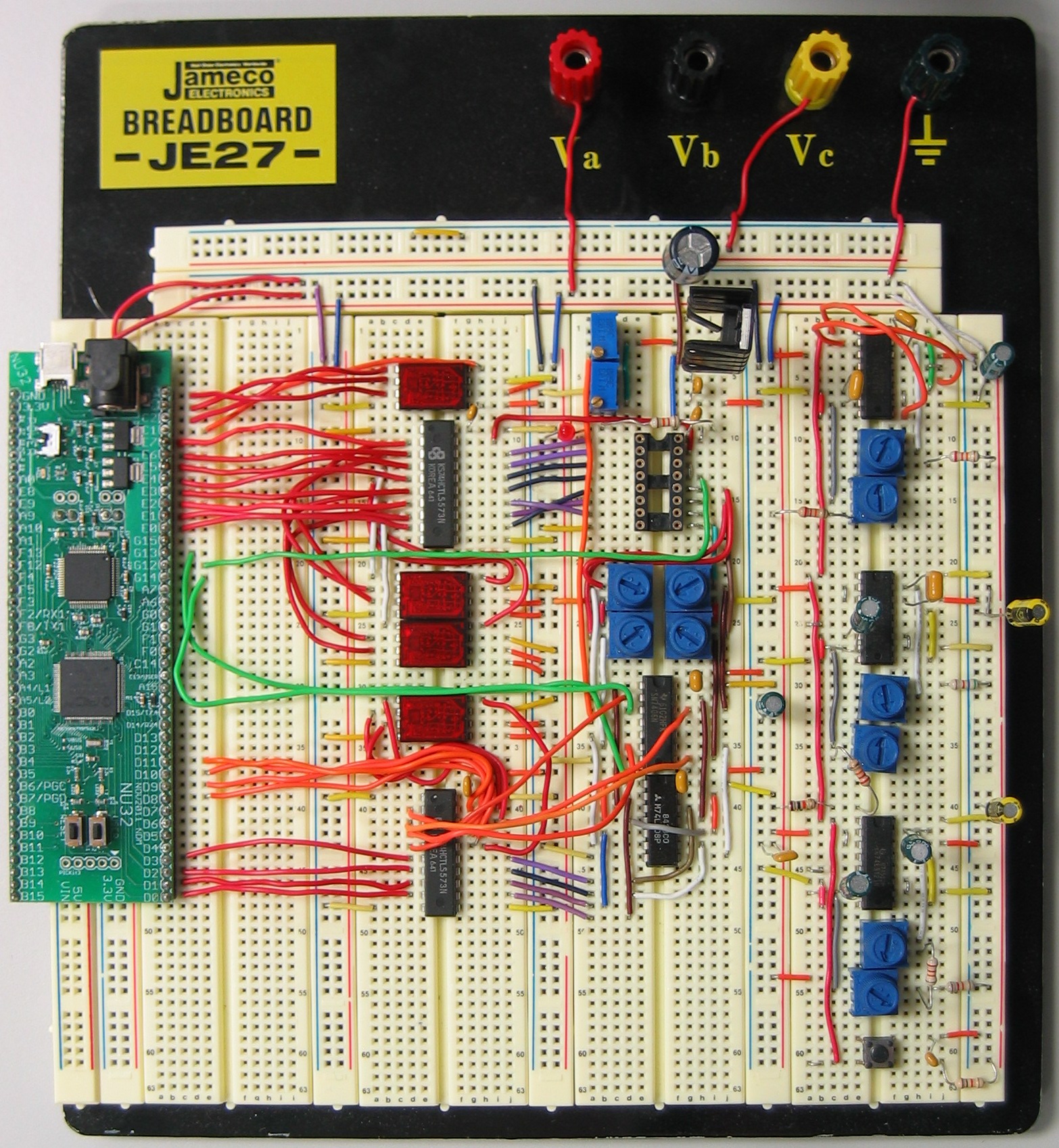
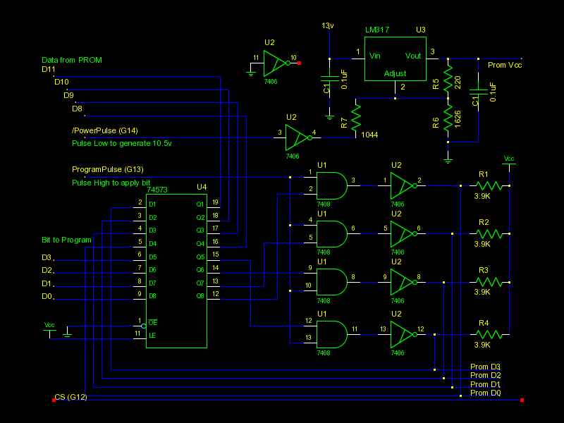
Consequently, I pulled a board built around a Microchip PIC32 processor from my junk box and connected it to the breadboard. It was overkill for this project, but had lots of I/O pins and was easy to interface with a laptop. I had never used it before, and this seemed like a good time to play with something new.
I used a pair of latches to buffer the address and data signals between the PROM and programmer logic. The programming voltage adjustment is handled by an adjustable voltage regulator. One of the pins on the PIC32 was connected through an open collector inverter to a resistor to adjust the voltage output which was in turn connected to the PROM chip’s power supply.
The programming bits were also supplied through open collector inverters, to ensure that the correct resistance is applied to the pins not being programmed while grounding the programmed pin.
SN74S287 Programmer Schematic
The schematic illustrates how the latch was used to buffer the data pins. An inverter was selected to adjust the voltage regulator as it ensures that the voltage is set to 5v when the PIC32 is powered on. This avoided applying 10.5v to the PROM being programmed while the circuit was initializing.
The resistance values were calculated and then verified by using ngspice to simulate the voltage adjustment circuit before installing it on the breadboard. By using potentiometers, the resistance was carefully adjusted to ensure that the voltages applied were correct by manually setting the programming select line high and then low.
The PIC32 was programmed with a simple program to appear as a serial device. It responded to an address set, data set, bit select, and program commands. After each command it responded with the current status of each port. The program command handles the timing for the chip select and program lines, ensuring that the timing follows the specifications on the data sheet.
A small script interfaced with the PIC32 through the virtual serial interface. The script started by reading in the data to be programmed. For each 4 bits of data, the script sets the address and data, and then steps through the bits that required programming, applying a program pulse for each one. Bits set to zero were programmed, and bits set to one were left in their default state.
As the circuit appeared as a serial port, I used a terminal program for testing. I sent the initial commands one at a time to view the resulting voltages and signals. By stepping through the commands, I was able to fine tune the various resistors required to obtain the correct programming voltages. This process also allowed me to program the first few data values by hand to observe the results slowly and ensure that the circuit was operating correctly.
In the video below, you can see the address selected (middle two values), current state of the bits in the PROM (on the left), and the desired final state (on the right.) If you watch carefully you can see as the original F state of the PROM is adjusted to the final state one bit at a time.
At VCF East this spring I demonstrated one of my vintage computer systems. My table was placed between two individuals using switches to enter software on their systems.
I was greatly intrigued by this idea, as I had never had a system that could be operated at such a low level.
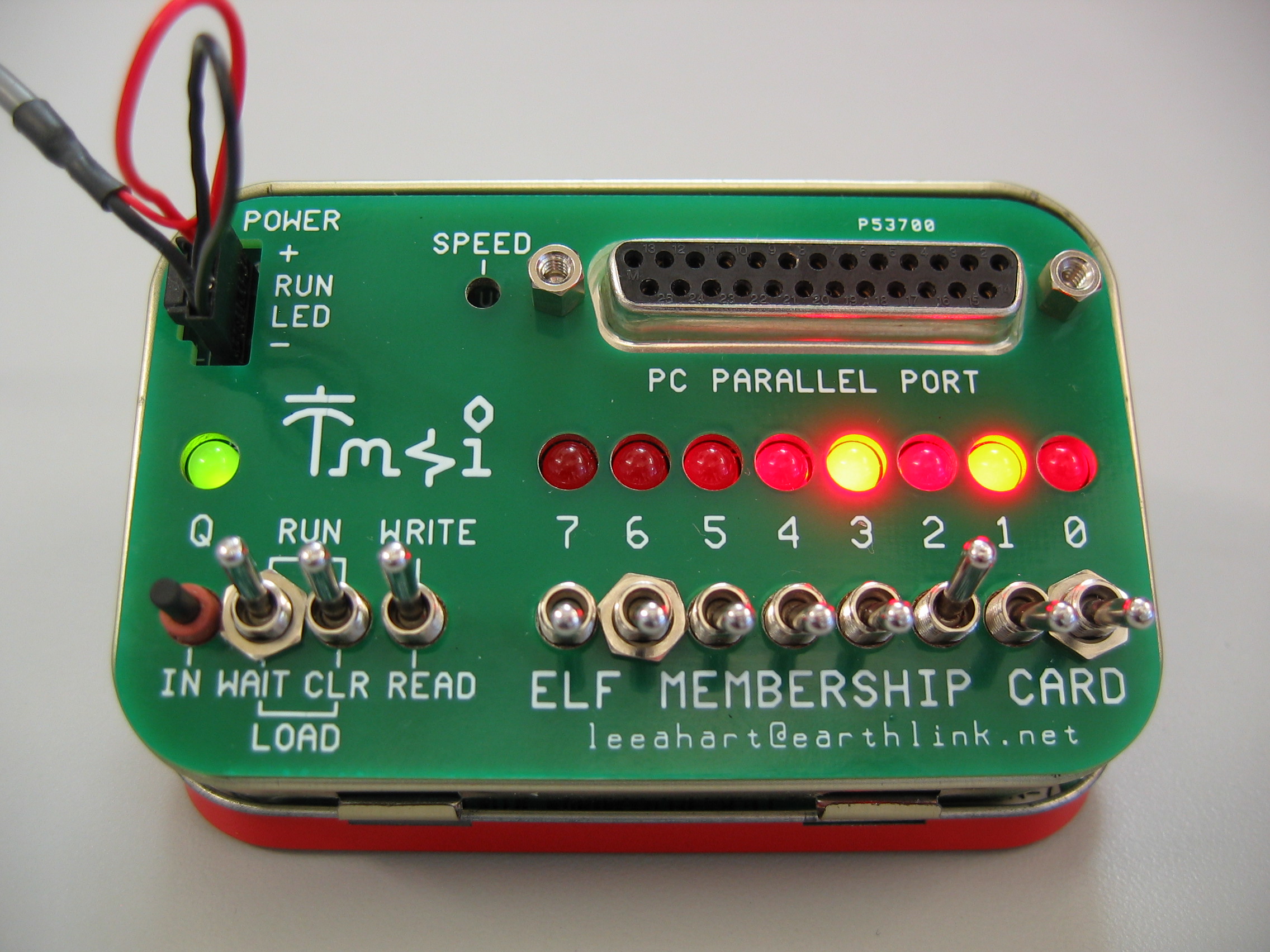
When I heard that a large exhibit around the COSMAC (RCA 1802) processor would be at VCFMW, I considered that this would be an excellent time to assemble one of the Elf Membership Card kits in order to understand what the systems were all about.
After packing for VCFMW a day early, I found myself with some time the day before. I dug out the membership card, and looked for something interesting to do with a short program and the lights on the front.
I considered a number of things before doing some research into Conway’s Game of Life. Normally a 2D cellular automaton, I wondered if perhaps there wasn’t a 1D form. This led me to Rule 90, which describes the operation of a one dimensional “life form.”
Rule 90 can be characterized by one simple rule.
If a cell has one and only one live neighbor cell, it will be alive in the next generation.
Initially, I considered the complexity of processing each bit at a time, but quickly realized that this is the XOR of the neighbor bits. As a result, the computation of all the bits can be easily implemented by computing the XOR of the current state shifted left once, and right once. This can be easily implemented by the below program.
The program reads the state of the switches as the initial state of the automaton. It then displays each generation on the LEDs.
00:     90	GHI     R0
01:     B1	PHI     R1
02:     F8 F0   LDI     F0  ; Temp
04:     A1	PLO     R1
05:     E1	SEX     1
06:     6C	INP     4
07:     A2	PLO     R2  ; Loop: Save current
08:     F6	SHR
09:     51	STR     R1  ; Save shifted right
0A:     F8 02   LDI     02
0C:     B3	PHI     R3
0D:     23      DEC     R3  ; Wait
0E:     93	GHI     R3
0F:     3A 0D   BNZ     Wait
11:     82	GLO     R2  ; Get current state
12:     FE	SHL         ; Shift left
13:     F3	XOR         ; XOR shifted right
14:     51	STR     R1  ; Save result
15:     64	OUT     4
16:     21	DEC     R1
17:     30 07   BR	Loop

F0:     00                  ; Temp