All posts by Christopher

A Tale of Switches

Switches with logos
Switches with logos
Switch backs
Switch backs

While working on my mini OSI-300 Trainer, I encountered issues with the switches that I had purchased.  The seller advertised them as SS12D07 switches, which according to the data sheets that I had found, were non-shorting, single pole, double throw switches.

They were single throw, double pole, and fit the size and shape specifications.  Unfortunately, the ones I received were definitely not non-shorting, otherwise known as break before make, switches.  I found a single SS12D02 from Jameco in among my assortment of switches.  It appears to be non-shorting, and taking it apart I found that it uses a slightly different mechanism than the SS12D07 I had purchased.

I placed an order for C&K OS102011MS2QN1 switches, which are designed to be non-shorting (there is a specific shorting version.)   The C&K parts arrived and I have tested and confirmed that they are definitely non-shorting as expected.

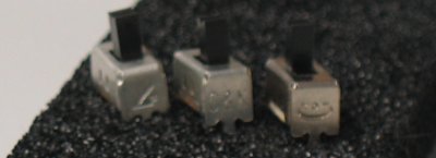
In the images above, I show the parts from left to right:

  • Jameco SS12D02
  • C&K OS102011MS2QN1
  • T.O.Y SS12D07 (shorting)

Both the Jameco and C&K parts have two small vertical slots on the side.  The T.O.Y part has an indentation on the opposite side, which can be seen in the second image.

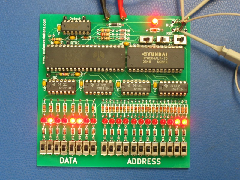
For my mini OSI-300, the T.O.Y parts are usable for all but the Run and Reset switches.  The Data and Address switches are configured as single pole, single throw.  The NMI switch has a resistor to prevent a direct short to ground, and the ROM switch does not switch between power and ground directly.  The Load switch is configured as a double pole, single throw switch as well.

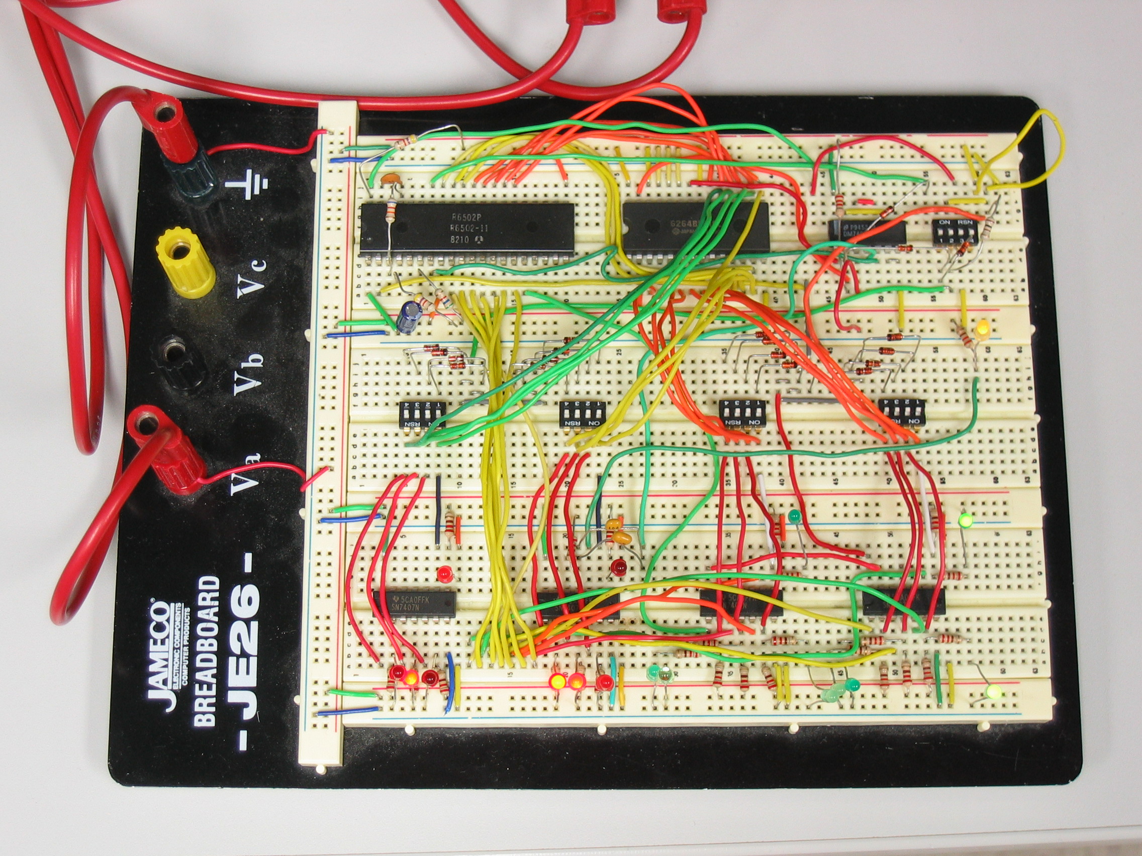
In general, I have had the expected results when purchasing parts from places other than the big parts houses such as Mouser, Digi-key, Jameco, etc.  I find that looking closely at images and reviews improves the odds of receiving a working part.  Out of the ten 6264 SRAM chips I received, although all were marked with the same markings on top, they all had different tool marks on the body, markings on the backside, and three were completely non-functional.


Completed OSI-300 mini prototype

Completed PrototypeAs indicated in my previous posting, I had issues with the switches that I purchased and their usage in the OSI-300 mini.  I took apart one of the switches in order to get a closer look at how it worked and if the switch could be adjusted to work properly for my application.

The switch has three blades that are made as extensions to the individual leads.  The switch connection is made by a metal slider that has four contact points, two on each side of the blades.  These contact points are supposed to be sized such that they do not contact the outer two blades at the same time.  The options to fix this are to separate the blades with more space, or shorten the contact points to avoid shorting the outer blades.

I looked at a similar component at work and found that they had shortened the slider slightly by bending the outside corners of the four contacts.  I took a pliers and did the same to two of the switches that I had.  After much trial and error, I was able to adjust the switch to prevent the shorting that I had seen.  I soldered them in place to complete the prototype and took the image above.


Prototype OSI-300 mini

Prototype mini-trainer

I recently received the boards I designed from the manufacturer.  They were very well done, even with the tight tolerances required to line up the various components.

Additionally, the parts I ordered to assemble the board arrived as well, and I set to assembling the board.

After a few hours of soldering, I was able to come up with the attached image.  I ran into only two issues, one with the design, and one with the parts.

The schematic I drew had an issue with the connection between the resistor and capacitor that form the clock circuit.  After a single trace was cut and a short piece of wire was attached, I had a working clock.

The other issue I ran into involved the switches in the RUN and RST positions.  Both of these switches switch a signal between power and ground.  While the switches I picked were supposed to be non-shorting, they appear to briefly short when switched.  As a result, power is connected to ground, and the contents of the SRAM are lost.  I will try a different manufacturer and see if their switches perform better.

To avoid this, using a pull up or down resistor would be a better design.  I wanted to keep as close to the original design as possible.

The image above shows the board running a simple JMP 0000 loop at address 0000.  The data LEDs represent 01001100, or 4C in hex, the command for a jump.  The address LEDs represent 00000011, or a merge of addresses 0, 1, and 2.  While the LEDs are flashing, they are doing so too quickly to see.

OSI-300 (Mini) PCB design

OSI-300 (mini)After playing with Kicad, and particularly with pcbnew, I have worked out a PCB design for a “mini” version of the OSI-300 trainer.  Only a few changes have been made to the original design.

The primary adjustment is to swap a 6264 SRAM for the original 128 byte 6810 SRAM.  This provides for 8k of space, and allows for more flexibility in that it will also accept a 62256, or with a trace cut and wire adjustment, a 6116.  This also permits the replacement of the SRAM with an NVRAM.

I also added 5 additional switches to the address bus.  This uses 5 gates on the 7417 open collector buffer chips, which were originally unused.  With 12 address bits, 4k is available for programming.

OSI-300 Trainer

OSI-300 Trainer Breadboard VersionThe OSI Model 300 Computer Trainer was advertised by Ohio Scientific Instruments in 1976 as a computer designed to  introduce individuals to computers and teach them the basics of programming the MOS 6502 processor.  The original trainer consists of a MOS 6502 processor,  6810 128 byte static RAM, one bit output latch, switches for entering data, and LEDs for reading the values of RAM.

The trainer was intended as a starter for individuals before moving on to their more advanced Model 400 Superboard system.

I first encountered one of these at VCFE 9.1 in 2014, and was intrigued by the simplicity of the design.  I was particularly interested in the operation, and wanted to learn how the switches and LEDs were interfaced to perform the data read/write operations.

OSI-300 Trainer Breadboard Version (Top View)
With the assistance of multiple individuals and lots of looking at images, I’ve worked out the schematic for the original and assembled it on a breadboard.

I did make one small change, using a 8k by 8-bit 6264 static RAM chip.  As this chip is larger than the original 6810, I added an additional address line for 256 bytes of accessible space.  The basic design could be expanded to the full 64k space.

The image shows the results running Experiment 3, which is a basic program that merely loops at location 0.  The red LEDs indicate the data, the green the address, and the yellow the run status.  If you look closely, you will see the green LEDs represent binary 11, which is because the loop uses locations 00, 01, and 10.  The data LEDs represent 01001100, as the 6502 jump instruction is 01001100.  The other two locations (01 and 10) both contain 00000000, which represents the location to which the program should jump.

There are several interesting design decisions made to keep the parts count and price down.  The first is the usage of a resistor and capacitor to act as the clock.  This takes advantage of the internal clock generator on the 6502.

The four buffer chips (7407/7417) provide multiple purposes.   For the data lines, they act as drivers for the data LEDs and the run LED.  For the address lines, they buffer the lines with the outputs driving both the address LEDs and the address lines for the RAM.  The power to the address buffers is only turned on when the RUN switch is active.  This in effect tri-states the address lines when the RUN switch is disabled, allowing the switches to drive the address lines without interference from the CPU.  This is because the 6502 is incapable of releasing the address lines.

The final chip, a 7402 (quad NOR,) inverts the SYNC line, driving an RC network to stretch it, before it is finally buffered to drive the run LED.  Two of the gates form a basic SR latch controlled by the address lines for page 1 and page 2.  I used the last NOR gate as an inverter for between the SRAM’s OE and R/W pins.

In the schematic I have generated, the diodes are likely 1N914 or similar with the exception of D35, which is intended for reverse polarity.  It is most likely a 1N4001.  I have left off the bypass capacitors for clarity.  They are likely .2uF on the trainer.

June 19, 2015: I have updated the schematic with a minor correction to the connection of the resistor forming the clock circuit.

Schematic: http://randomvariations.com/wp-content/uploads/2015/05/trainer.pdf

January 1977 Byte Article: https://archive.org/stream/byte-magazine-1977-01/1977_01_BYTE_02-01_Hash_Tables_and_Interrupts#page/n95/mode/2up