Category Archives: Verifone Omni 396

N8VEM test0

N8VEM test0
N8VEM test0

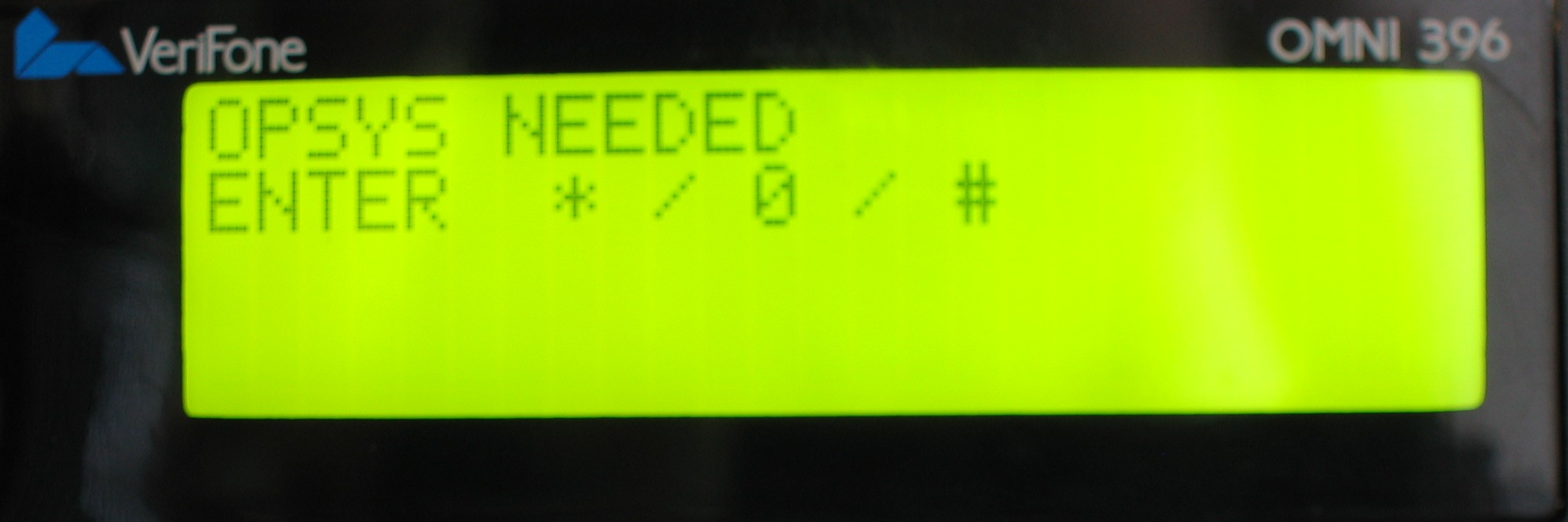
I needed a simple program to send hello to the world and indicate that my code was operating in place of the original Verifone terminal.

I searched online for an open source project working with hardware similar to my own.  Fortunately, the N8VEM project is working on just a system, called the Mark IV.

Even more fortunately, their basic test routines had been recently uploaded.  After reconfiguring the I/O locations to match the credit card terminal, and implementing a bit of slight of hand to ensure that the firmware matched the critical signature bytes of the original, I was ready to upload it to the terminal.

While running my program, I watched as the terminal counted the blocks my program sent to be stored in the flash.  After a few reset and adjustment cycles, I was able to connect a terminal program to the credit card terminal and observe the test routine’s output.  I had succeeded in running the test code, as I observed the “Hello World!” output on my screen.

This had been a lengthy process, but I wasn’t done yet.  I wanted to run a real operating system on it, and most of all, run Zork!

Download Old Firmware, Upload It Back

Upload/Download Prompt

Now that I had reached the upload/download prompt,  I needed to configure my laptop to receive the current firmware from the credit card terminal.

This step involved carefully tracing  the start-up firmware of the credit card terminal.  At the same time, I was building a program to send the responses required to emulate another Verifone Omni 396 waiting for a new firmware image.

Once the download protocol was documented, the process was reversed.  At first, I wrote a program to send the same firmware back to the originating terminal.  I could do this by just sending back the data I had just captured.

However, to send my own firmware, I needed to calculate the correct checksums for each packet, and the final checksum for the firmware CRC for it to activate.

Fortunately, the packet checksum was the common Verifone standard checksum used by previous products.  Calculating the firmware checksum was a simple sum placed into the correct position in the firmware.

Now, I had the ability to reprogram the unit, but what to program as a simple test case?


Operating Firmware

Firmware Dump
Firmware Dump

With the correct configuration on the logic analyzer, I was now able to capture the bytes from the firmware as they were checked by the CRC routine.

With a depth of only 1024 bytes, this took some time, but each capture was printed to my laptop.

A small script later, and I converted these into a binary dump of the firmware for disassembly.

Even though this didn’t give me the start-up firmware, it did give me useful tools to build that firmware as I captured traces with the logic analyzer.  As I worked my way through the initialization sequence, each trace performed was saved to the laptop, and all the traces were merged together to create an image that could be used concurrently in a disassembler.

Finally, I worked my way down through the initial sequence of keys used to navigate to the upload and download routines.  At this point, the terminal was displaying a prompt asking if I wanted it to send or receive the firmware.

Disassembling Code

Manual DisassemblyInitially, I sat with the logic analyzer, entering each address and byte into a text file, as I followed the start-up sequence of the credit card terminal.  This was a time consuming method, but it gave me excellent training into how the logic analyzer and the credit card terminal worked.

After all, learning was what this project was about!  While doing things “the hard way” is often difficult, it tends to make for a much more rewarding and memorable experience.

As I progressed through the code and grew more experienced, I switched to having the logic analyzer “print” the data recorded through a serial port to my laptop.  This was considerably easier than retyping each byte.  As I followed the normal start-up sequence, I made a very useful discovery.

The terminal ran a CRC check on the firmware stored in flash!


Logic Analyzer Connection

Logic Analyzer Connection

This image shows the final results from carefully tracing the pins from the flash chip back to the other chips in the credit card terminal.  Through this connection, I was able to view the address and data lines as they were connected to the flash chip, along with the important select lines.  I also added connections to the write line and chip enable lines for the main memory.   Exposing these connections would give me a method of capturing the data not only from flash, but memory as well.  The extra signals would make it possible to differentiate between the accesses to the two chips.

With this in place, I was ready to start.  I configured the logic analyzer to store the data and address lines when the flash or memory was accessed, along with the read/write status line.  I set the logic analyzer to run mode, and inserted the plug to power up the credit card terminal.

The results were immediate.  There on the screen was the code currently running, starting at address 0.  The following bytes were the program as it proceeded to initialize the hardware.

I had a long task ahead of myself, but, at least now, I could see inside the system to visualize how the terminal operated.